- 您现在的位置:买卖IC网 > Sheet目录39251 > LMX2532LQX1065/NOPB (NATIONAL SEMICONDUCTOR CORP) PLL FREQUENCY SYNTHESIZER, 19.68 MHz, QCC28
Programming Description
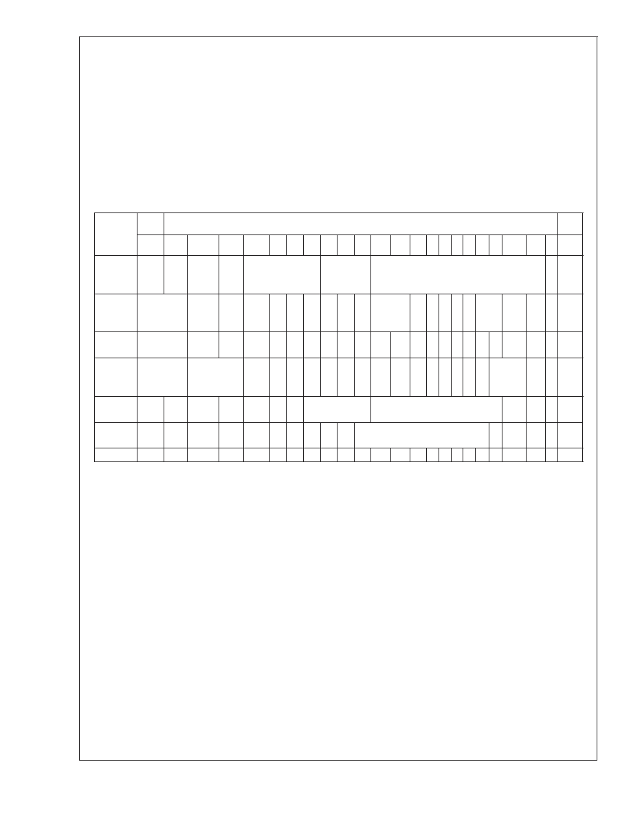
CONTROL REGISTER CONTENT MAP
The serial interface has a 24-bit shift register to store the incoming data bits temporarily. The incoming Data is loaded into the shift
register from MSB to LSB. The Data is shifted at the rising edge of the Clock signal. When the Latch Enable signal transitions from
LOW to HIGH, the data stored in the shift register is transferred to the proper register depending on the address bit settings. The
selection of the particular register is determined by the control bits indicated in boldface text.
At initial start-up, the MICROWIRE loading requires 4 default words (registers R3, loaded first, to R0, loaded last). After the device
has been initially programmed, the RF VCO frequency can be changed using a single register (R0). If an IF frequency other than
the default value for the device is desired the SPI_DEF bit should be set to 0, the desired values for IF_A, IF_B, and IF_R entered
and words R6 to R0 should be sent.
The control register content map describes how the bits within each control register are allocated to the specific control functions.
Complete Register Map
Register
MSB
SHIFT REGISTER BIT LOCATION
LSB
23
22
21
20
19
18 17 16 15 14 13 12
11
10 98765
4
3
2
1 0
R0
(Default)
SPI_
DEF
RF_
SEL
RF_
LD
SP
UR_
CRL
RF_B
[3:0]
RF_A
[2:0]
RF_FN
[10:0]
00
R1
(Default)
IF_
FREQ
[1:0]
OSC_
FREQ
1
0
000000
SPUR_
RDT
[1:0]
0
0101OB_
CRL
[1:0]
RF_
EN
IF_
EN
01
R2
(Default)
IF_
CUR[1:0]
0
1
0011101
1
0
10100
0
1
0
10
R3
(Default)
BW_
DUR
[1:0]
BW_
CRL
[1:0]
BW_
EN
1011110
1
0
00110
VCO_
CUR
[1:0]
01 1
R4
0
1
0
IF_A
[3:0]
IF_B
[8:0]
01
1 1
R5
0
1
0
00010
IF_R
[8:0]
01
1
1 1
R6
1
0
0000000
0
0000 011
1
1 1
NOTE: Bold numbers represent the address bits.
LMX2522/LMX2532
www.national.com
10
发布紧急采购,3分钟左右您将得到回复。
相关PDF资料
LMX2532LQX0967/NOPB
PLL FREQUENCY SYNTHESIZER, 19.68 MHz, QCC28
LMX2522LQX1635/NOPB
PLL FREQUENCY SYNTHESIZER, 19.68 MHz, QCC28
LNB003-01GT
SIP3, IC SOCKET
LNB003-29GT
SIP3, IC SOCKET
LNB003-29TT
SIP3, IC SOCKET
LNB003-49GG
SIP3, IC SOCKET
LNB003-51TT
SIP3, IC SOCKET
LNB004-01TT
SIP4, IC SOCKET
相关代理商/技术参数
LMX2541
制造商:NSC 制造商全称:National Semiconductor 功能描述:Ultra-Low Noise PLLatinum Frequency Synthesizer with Integrated VCO
LMX25412060EVAL
功能描述:时钟和定时器开发工具 LMX25412060 EVAL BOARD
RoHS:否 制造商:Texas Instruments 产品:Evaluation Modules 类型:Clock Conditioners 工具用于评估:LMK04100B 频率:122.8 MHz 工作电源电压:3.3 V
LMX25412060EVAL/NOPB
功能描述:时钟和定时器开发工具 LMX25412060 EVAL BOARD
RoHS:否 制造商:Texas Instruments 产品:Evaluation Modules 类型:Clock Conditioners 工具用于评估:LMK04100B 频率:122.8 MHz 工作电源电压:3.3 V
LMX25412380EVAL/NOPB
功能描述:时钟和定时器开发工具 LMX25412380 EVAL BOARD
RoHS:否 制造商:Texas Instruments 产品:Evaluation Modules 类型:Clock Conditioners 工具用于评估:LMK04100B 频率:122.8 MHz 工作电源电压:3.3 V
LMX25412690EVAL/NOPB
功能描述:时钟和定时器开发工具 LMX25412690 EVAL BOARD
RoHS:否 制造商:Texas Instruments 产品:Evaluation Modules 类型:Clock Conditioners 工具用于评估:LMK04100B 频率:122.8 MHz 工作电源电压:3.3 V
LMX25413030EVAL/NOPB
功能描述:时钟和定时器开发工具 LMK2541SQ3030 EVAL KIT
RoHS:否 制造商:Texas Instruments 产品:Evaluation Modules 类型:Clock Conditioners 工具用于评估:LMK04100B 频率:122.8 MHz 工作电源电压:3.3 V
LMX25413320EVAL/NOPB
功能描述:时钟和定时器开发工具 LMK2541SQ3320 EVAL KIT
RoHS:否 制造商:Texas Instruments 产品:Evaluation Modules 类型:Clock Conditioners 工具用于评估:LMK04100B 频率:122.8 MHz 工作电源电压:3.3 V
LMX25413740EVAL/NOPB
功能描述:时钟和定时器开发工具 LMX25413740 EVAL BOARD
RoHS:否 制造商:Texas Instruments 产品:Evaluation Modules 类型:Clock Conditioners 工具用于评估:LMK04100B 频率:122.8 MHz 工作电源电压:3.3 V